
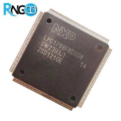


میکروکنترلر LPC1788FBD208 تایوان اورجینال
تراشه LPC1788 از سری پردازنده قوی شرکت NXP
ارسال پستی رایگان برای سفارشات
بیشتر از یـک مـیـلیـــون تــــومـــان.

Features and benefits
Functional replacement for the LPC23xx and LPC24xx family devices.
System:
ARM Cortex-M3 processor, running at frequencies of up to 120 MHz. A Memory
Protection Unit (MPU) supporting eight regions is included.
ARM Cortex-M3 built-in Nested Vectored Interrupt Controller (NVIC).
LPC178x/7x
32-bit ARM Cortex-M3 microcontroller; up to 512 kB flash and
96 kB SRAM; USB Device/Host/OTG; Ethernet; LCD; EMC
Rev. 5.5 — 26 April 2016 Product data sheet
LPC178X_7X All information provided in this document is subject to legal disclaimers. © NXP Semiconductors N.V. 2016. All rights reserved.
Product data sheet Rev. 5.5 — 26 April 2016 2 of 126
NXP Semiconductors LPC178x/7x
32-bit ARM Cortex-M3 microcontroller
Multilayer AHB matrix interconnect provides a separate bus for each AHB master.
AHB masters include the CPU, USB, Ethernet, and the General Purpose DMA
controller. This interconnect provides communication with no arbitration delays
unless two masters attempt to access the same slave at the same time.
Split APB bus allows for higher throughput with fewer stalls between the CPU and
DMA. A single level of write buffering allows the CPU to continue without waiting for
completion of APB writes if the APB was not already busy.
Cortex-M3 system tick timer, including an external clock input option.
Standard JTAG test/debug interface as well as Serial Wire Debug and Serial
WireTrace Port options.
Embedded Trace Macrocell (ETM) module supports real-time trace.
Boundary scan for simplified board testing.
Non-maskable Interrupt (NMI) input.
Memory:
Up to 512 kB on-chip flash program memory with In-System Programming (ISP)
and In-Application Programming (IAP) capabilities. The combination of an
enhanced flash memory accelerator and location of the flash memory on the CPU
local code/data bus provides high code performance from flash.
Up to 96 kB on-chip SRAM includes:
64 kB of main SRAM on the CPU with local code/data bus for high-performance
CPU access.
Two 16 kB peripheral SRAM blocks with separate access paths for higher
throughput. These SRAM blocks may be used for DMA memory as well as for
general purpose instruction and data storage.
Up to 4032 byte on-chip EEPROM.
LCD controller, supporting both Super-Twisted Nematic (STN) and Thin-Film
Transistors (TFT) displays.
Dedicated DMA controller.
Selectable display resolution (up to 1024 768 pixels).
Supports up to 24-bit true-color mode.
External Memory Controller (EMC) provides support for asynchronous static memory
devices such as RAM, ROM and flash, as well as dynamic memories such as single
data rate SDRAM with an SDRAM clock of up to 80 MHz.
Eight channel General Purpose DMA controller (GPDMA) on the AHB multilayer
matrix that can be used with the SSP, I2S, UART, CRC engine, Analog-to-Digital and
Digital-to-Analog converter peripherals, timer match signals, GPIO, and for
memory-to-memory transfers.
Serial interfaces:
Ethernet MAC with MII/RMII interface and associated DMA controller. These
functions reside on an independent AHB.
USB 2.0 full-speed dual-port device/host/OTG controller with on-chip PHY and
associated DMA controller.
Five UARTs with fractional baud rate generation, internal FIFO, DMA support, and
RS-485/EIA-485 support. One UART (UART1) has full modem control I/O, and one
UART (USART4) supports IrDA, synchronous mode, and a smart card mode
conforming to ISO7816-3.
Three SSP controllers with FIFO and multi-protocol capabilities. The SSP
controllers can be used with the GPDMA.
LPC178X_7X All information provided in this document is subject to legal disclaimers. © NXP Semiconductors N.V. 2016. All rights reserved.
Product data sheet Rev. 5.5 — 26 April 2016 3 of 126
NXP Semiconductors LPC178x/7x
32-bit ARM Cortex-M3 microcontroller
Three enhanced I2C-bus interfaces, one with a true open-drain output supporting
the full I2C-bus specification and Fast-mode Plus with data rates of 1 Mbit/s, two
with standard port pins. Enhancements include multiple address recognition and
monitor mode.
I2S-bus (Inter-IC Sound) interface for digital audio input or output. It can be used
with the GPDMA.
CAN controller with two channels.
Digital peripherals:
SD/MMC memory card interface.
Up to 165 General Purpose I/O (GPIO) pins depending on the packaging with
configurable pull-up/down resistors, open-drain mode, and repeater mode. All
GPIOs are located on an AHB bus for fast access and support Cortex-M3
bit-banding. GPIOs can be accessed by the General Purpose DMA Controller. Any
pin of ports 0 and 2 can be used to generate an interrupt.
Two external interrupt inputs configurable as edge/level sensitive. All pins on port 0
and port 2 can be used as edge sensitive interrupt sources.
Four general purpose timers/counters with a total of eight capture inputs and ten
compare outputs. Each timer block has an external count input. Specific timer
events can be selected to generate DMA requests.
Quadrature encoder interface that can monitor one external quadrature encoder.
Two standard PWM/timer blocks with external count input option.
One motor control PWM with support for three-phase motor control.
Real-Time Clock (RTC) with a separate power domain. The RTC is clocked by a
dedicated RTC oscillator. The RTC block includes 20 bytes of battery-powered
backup registers, allowing system status to be stored when the rest of the chip is
powered off. Battery power can be supplied from a standard 3 V lithium button cell.
The RTC will continue working when the battery voltage drops to as low as 2.1 V.
An RTC interrupt can wake up the CPU from any reduced power mode.
Event Recorder that can capture the clock value when an event occurs on any of
three inputs. The event identification and the time it occurred are stored in
registers. The Event Recorder is located in the RTC power domain and can
therefore operate as long as there is RTC power.
Windowed Watchdog Timer (WWDT). Windowed operation, dedicated internal
oscillator, watchdog warning interrupt, and safety features.
CRC Engine block can calculate a CRC on supplied data using one of three
standard polynomials. The CRC engine can be used in conjunction with the DMA
controller to generate a CRC without CPU involvement in the data transfer.
Analog peripherals:
12-bit Analog-to-Digital Converter (ADC) with input multiplexing among eight pins,
conversion rates up to 400 kHz, and multiple result registers. The 12-bit ADC can
be used with the GPDMA controller.
10-bit Digital-to-Analog Converter (DAC) with dedicated conversion timer and
GPDMA support.
Power control:
Four reduced power modes: Sleep, Deep-sleep, Power-down, and Deep
power-down.
LPC178X_7X All information provided in this document is subject to legal disclaimers. © NXP Semiconductors N.V. 2016. All rights reserved.
Product data sheet Rev. 5.5 — 26 April 2016 4 of 126
NXP Semiconductors LPC178x/7x
32-bit ARM Cortex-M3 microcontroller
The Wake-up Interrupt Controller (WIC) allows the CPU to automatically wake up
from any priority interrupt that can occur while the clocks are stopped in
Deep-sleep, Power-down, and Deep power-down modes.
Processor wake-up from Power-down mode via any interrupt able to operate
during Power-down mode (includes external interrupts, RTC interrupt, PORT0/2
pin interrupt, and NMI).
Brownout detect with separate threshold for interrupt and forced reset.
On-chip Power-On Reset (POR).
Clock generation:
Clock output function that can reflect the main oscillator clock, IRC clock, RTC
clock, CPU clock, USB clock, or the watchdog timer clock.
On-chip crystal oscillator with an operating range of 1 MHz to 25 MHz.
12 MHz Internal RC oscillator (IRC) trimmed to 1% accuracy that can optionally be
used as a system clock.
An on-chip PLL allows CPU operation up to the maximum CPU rate without the
need for a high-frequency crystal. May be run from the main oscillator or the
internal RC oscillator.
A second, dedicated PLL may be used for USB interface in order to allow added
flexibility for the Main PLL settings.
Versatile pin function selection feature allows many possibilities for using on-chip
peripheral functions.
Unique device serial number for identification purposes.
Single 3.3 V power supply (2.4 V to 3.6 V). Temperature range of 40 C to 85 C.
Available as LQFP208, TFBGA208, TFBGA180, and LQFP144 package.
- نام برند
- NXP
- مدل
- LPC1788FBD208
- ساخت
- NXP Semiconductors
- بسته بندی
- SMD
- ولتاژ کاری
- 2.4V - 3.6V
- تعداد IO
- 165
- تعداد ورودی آنالوگ
- 12
- فرکانس
- 120MHz
- FLASH
- 512KB
- SRAM
- 96KB


 GOOI)")


